Designing a USB communications box.
Several of the projects we have been working on recently needed some form of serial communication with our PC, either through RS232, UART, I2C or SPI and at the moment we use a handful of different USB-to-serial adapters designed for each different protocol. One problem we have run into before is ground loops between the PC and the devices under test can occasionally cause problems. What we needed was a single communications box that works with all of the normal communications protocols and is isolated from the PC. After looking at some of the isolated USB to RS232 converters that are on the market we decided that we would build our own.
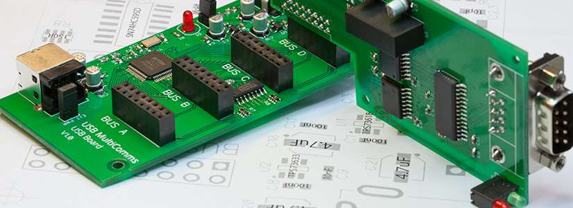
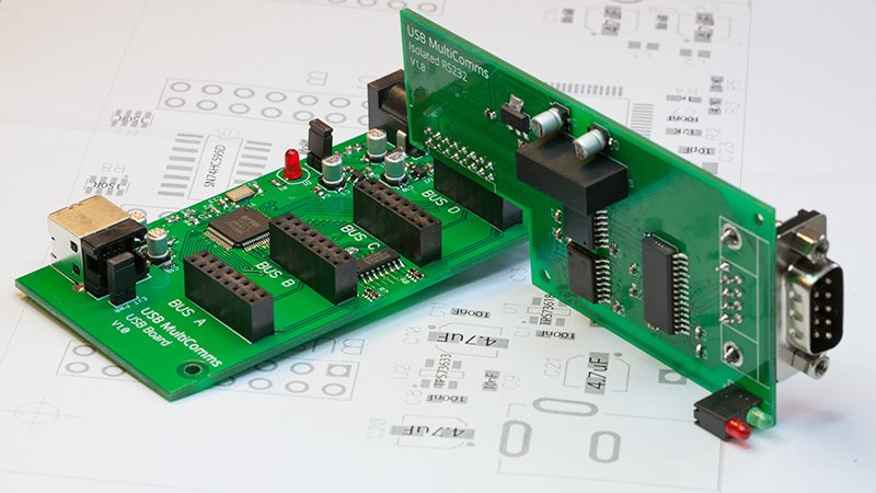
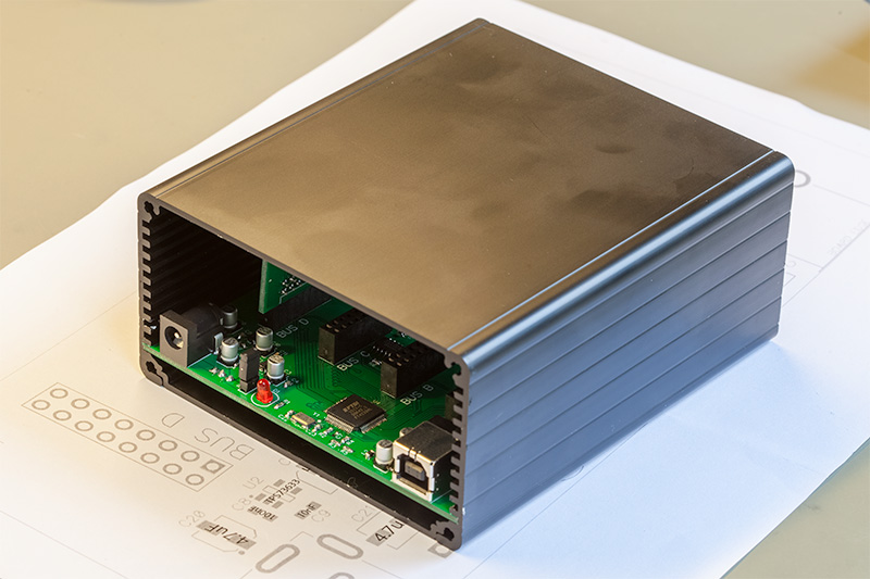
We came up with a few requirements for the new communications box. It had to support multiple serial protocols, the ports need to be isolated from the PC and it needs to be modular so we can build several boxes with different types of the serial port on the front. We decided that the best approach would be to build a main board with the USB to serial IC, USB port and power supply and then use separate daughter boards for each of the different serial protocols that we want to support. That way we could be one box with 4 RS232 ports or a box with 2 RS232 and 2 UART ports or one with an RS232, a UART, RS485 and a JTAG port, etc.
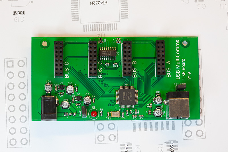

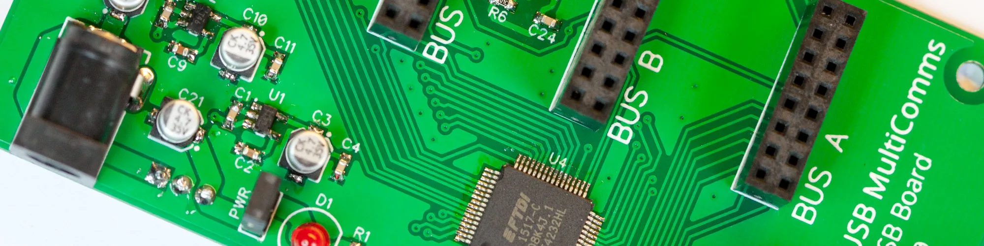
The main board is based around the FT4232H from FTDI. This chip supports up to 4 serial ports with two configurable JTAG, SPI, I2C or 8 general IO pins. The other two ports can be used for RS232, RS485, RS422 and UART. We based the circuit on the reference design from FTDI with power provided either from the PC's USB port or from an external supply through a 7805 regulator. This means that the current limit will be around 1A for the main board and daughter boards combined.
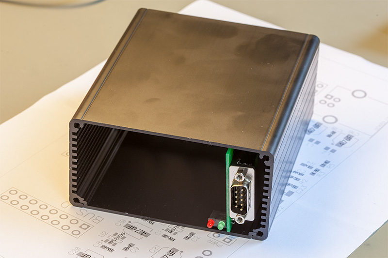
A suitable enclosure was found that uses extruded aluminium for the sides with plastic end plates so the connectors can be isolated from each other. We designed the main board so that it sits at the back of the case with the daughter boards plugged in vertically so you can have four daughter boards stacked 20mm apart across the enclosure.
So far we have designed the main board and RS232 one daughter board. The main board works perfectly and appears under Windows as four com ports.
When the PCB for the RS232 daughter board arrived we found that the connectors were backwards and the isolated switch-mode supply we used was a bit noisy so we are redesigning the daughter board with the connectors on the correct side and adding additional filtering on the power lines. Once the daughter boards are ready we will update the blog with our progress.
PCB design files for this project can be downloaded from https://github.com/briandorey/USB-MultiComms


Comments